


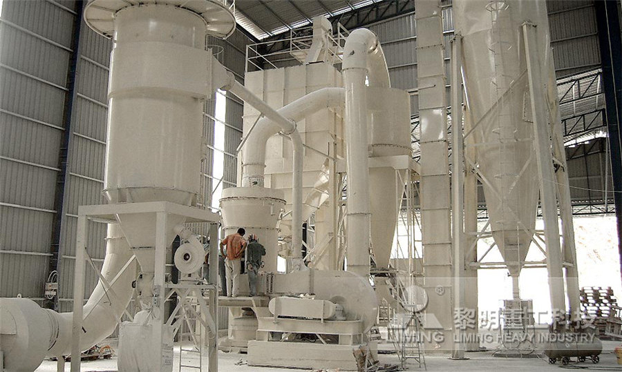
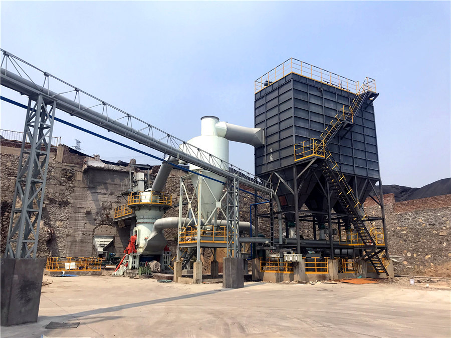
MTW European Type Trapezium Mill
Input size:30-50mm
Capacity: 3-50t/h
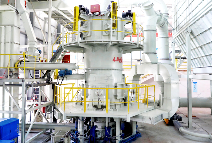
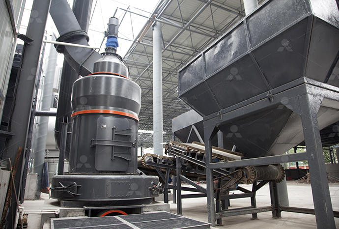
LM Vertical Roller Mill
Input size:38-65mm
Capacity: 13-70t/h
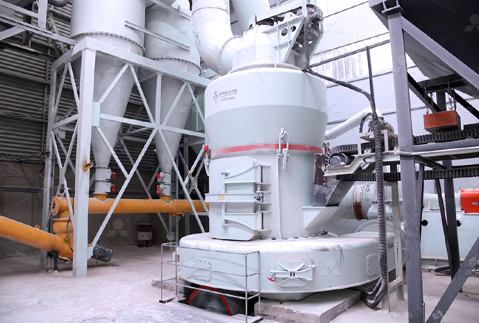
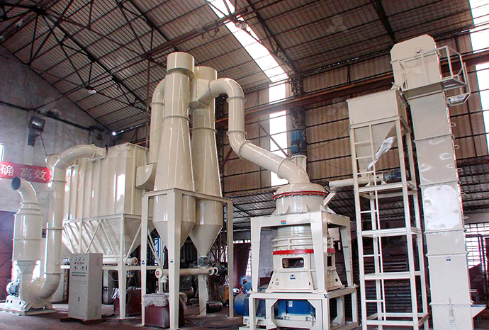
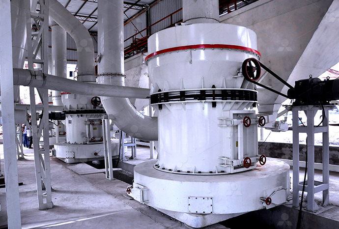
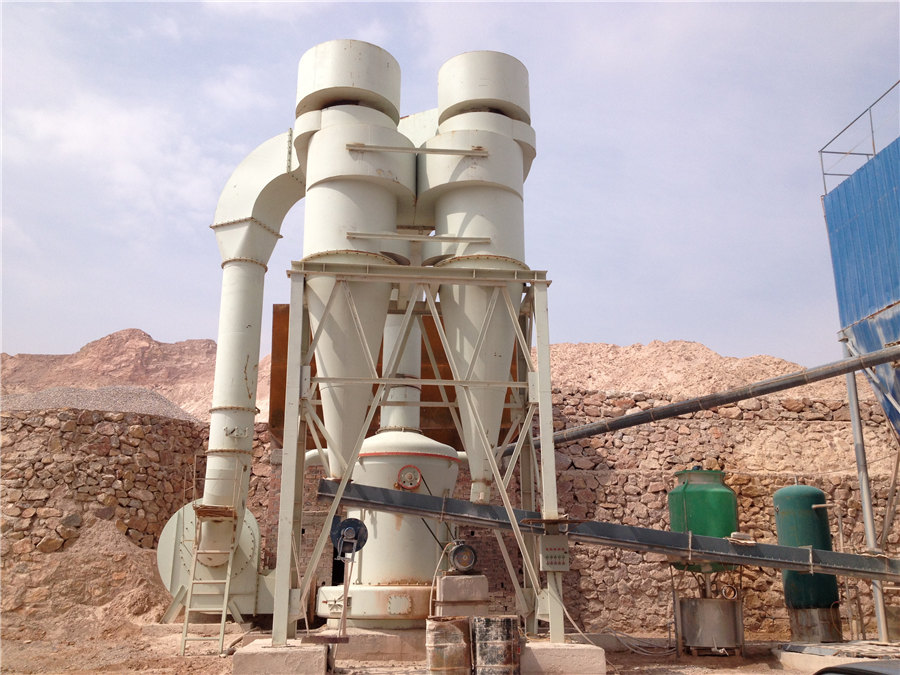
Raymond Mill
Input size:20-30mm
Capacity: 0.8-9.5t/h
Sand powder vertical mill
Input size:30-55mm
Capacity: 30-900t/h
LUM series superfine vertical roller grinding mill
Input size:10-20mm
Capacity: 5-18t/h
MW Micro Powder Mill
Input size:≤20mm
Capacity: 0.5-12t/h
LM Vertical Slag Mill
Input size:38-65mm
Capacity: 7-100t/h
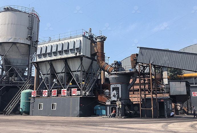
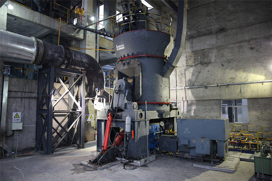
LM Vertical Coal Mill
Input size:≤50mm
Capacity: 5-100t/h
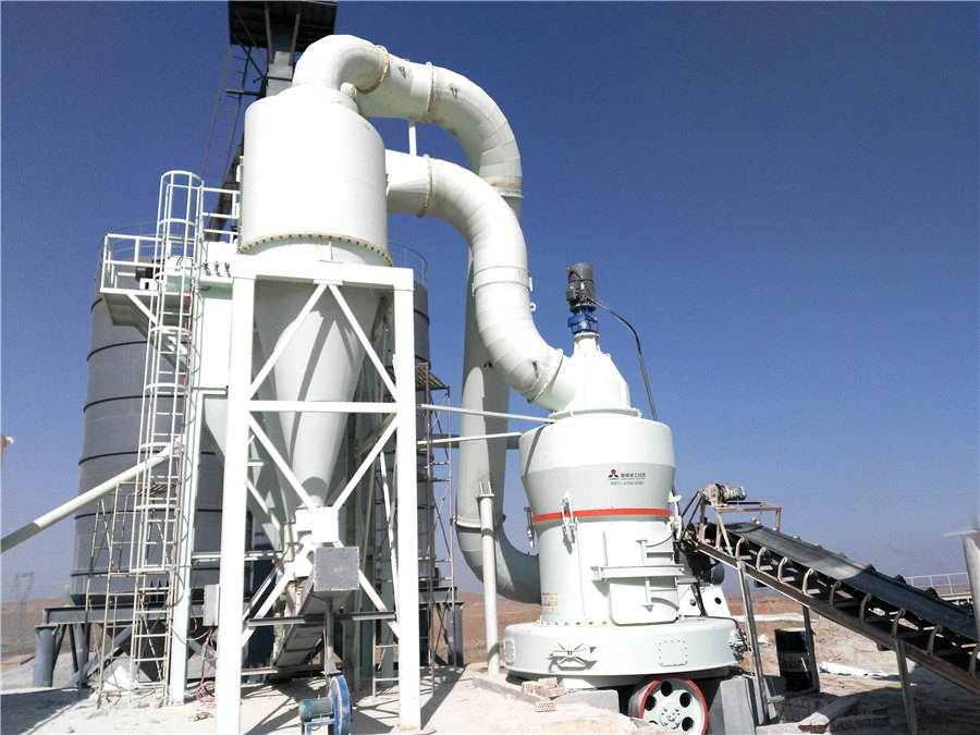
TGM Trapezium Mill
Input size:25-40mm
Capacity: 3-36t/h
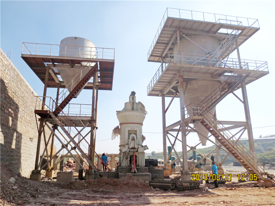
MB5X Pendulum Roller Grinding Mill
Input size:25-55mm
Capacity: 4-100t/h
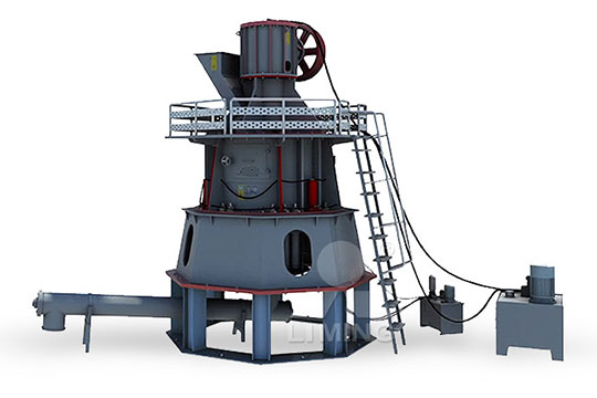
Straight-Through Centrifugal Mill
Input size:30-40mm
Capacity: 15-45t/h
Silicon equipment process flow
Semiconductor Manufacturing Process: Steps, Technology, Flow
2024年10月12日 In order for silicon to turn into a semiconductor chip, it needs to go through the several complex process of wafer manufacturing, oxidation, photolithography, etching, deposition and ion implementation, metal wiring, Eds and packaging Let’s take a closer look at this Silicon wafers are an important ingredient in manufacturing semiconductors ESD TSMC IndiaSemiconductor manufacturers are looking into 450mm diameter silicon wafers for use in the future Semiconductor devices are completed through the frontend process (wafer processing operation) and the backend process (assembly 1 Semiconductor manufacturing process : Hitachi High Owing to the superior properties of silicon carbide (SiC), such as higher breakdown voltage, higher thermal conductivity, higher operating frequency, higher operating temperature, and higherSiC MOSFET process flow Download Scientific
Silicon Wafer Manufacturing Process: Sand to Silicon
2024年9月7日 Silicon wafers are made through a process called Czochralski growth, where a silicon crystal is pulled from molten silicon and then sliced into thin wafers What are the key steps in silicon wafer fabrication?Single crystal silicon “seed” is placed into the melt and slowly rotated as it is “pulled out” Single crystalline ingot diameter is determined by a combination of temperature and extraction speed The Semiconductor Manufacturing Process Dalhousie University2023年10月4日 Let’s discuss six critical semiconductor manufacturing steps: deposition, photoresist, lithography, etch, ionization and packaging The process begins with a silicon wafer Wafers are sliced from a salamishaped bar of Six crucial steps in semiconductor manufacturing – The frontend fabrication process of the semiconductor silicon chips was classified into seven main processes: photolithography, etching, deposition, chemical mechanical planarization,Abstract process flow of typical semiconductor
.jpg)
An Introduction to Semiconductor Physics, Technology,
2014年10月9日 To make a computer chip, it all starts with the Czochralski process The first step of this process is to take extremely pure silicon and melt it in a crucible that is often made of quartzSemiconductors form the backbone of modern electronics, enabling the functionalities of devices we use daily This detailed exploration breaks down the semiconductor manufacturing process into its fundamental steps, mirroring the The Semiconductor Manufacturing Process: A Stepby 2024年11月21日 This equipment uses advanced technologies such as centrifugal force and pulsating water flow to separate silicon and iron ore particles effectively based on specific Optimizing Manganese Ore Process Flow and Siliconiron Ore Beneficiation Process EquipmentBack End(BE) Process Wafer Sawing(Dicing Saw) • Process by which individual silicon chips (die) are separated from each other on the wafer • Get the wafer cut per each lines with the DI(Deionized) water to prevent any electrostatic issue or contamination Silicon wafer Sawing blade Sawing blade Silicon wafer Before AfterIntroduction to Semico nductor Manufacturing and FA Process

Process Technology for Silicon Carbide Devices KTH
Silicon face Carbon face Silicon carbide is made up of equal parts silicon and carbon Both are period IV elements, so they will prefer a covalent bonding such as in the left figure Also, each carbon atom is surrounded by four silicon atoms, and vice versa This will lead to a highly ordered configuration, a single crystal, such as in the Download scientific diagram TSV interposer fabrication process integration flow from publication: Development of Through Silicon Via (TSV) Interposer Technology for Large Die (21x21mm) Fine TSV interposer fabrication process integration flowUnit processes, integration schemes, and equipment are in place to enable development and pilot production of TSV technologies and all parts of the value chain do exist today at 300mm to enable integration technology qualification, endproduct samples, and limited pilot production Sesh Ramaswami, Applied Materials, Santa Clara, CA USAProcess equipment readiness for throughsilicon via 2024年2月9日 In part 2, we went through all the various packaging technologies and their use casesIn part 3, we discussed Intel’s bet on thermocompression bonding (TCB) and the tool landscapeIn part 4 we talked about fanouts, organic interposers, and silicon bridges as a path past expensive passive interposers As the AI supply chain heated up, we also covered Hybrid Bonding Process Flow – Advanced Packaging Part 5
.jpg)
Semiconductor Fabrication Process: The Ultimate Guide to
2023年4月17日 Semiconductor Fabrication Process: The Ultimate Guide to Creating CuttingEdge Electronics Semiconductors have become an integral part of our modern lives that relies heavily on electronics, serving as the foundation for a wide range of such devices, from smartphones and computers to medical equipment, automotive applications, and renewable 2021年1月9日 Wafer manufacturing processes are also employed to produce photovoltaic wafers from single or polycrystalline silicon The generalized process flow of wafer manufacturing includes the following classification of four categories: crystal growth, wafer forming, wafer polishing, and wafer preparingWafer Manufacturing: Generalized Processes and FlowDownload scientific diagram Process flow of commercial HJT solar cells and key equipments SILEX II and GENERIS PVD provided by SINGULUS TECHNOLOGIES AG to the mass production from publication Process flow of commercial HJT solar cells and key equipments 2023年11月6日 Reliable liquid flow measurement plays an important role in semiconductor process management Flow meters can effectively monitor wet the process of photolithography describes the processing of circuit board designs on silicon wafers by means of light The process starts with coating the keep equipment uptime Increase manufacturing quality with reliable liquid flow
Semiconductor device fabrication Wikipedia
A diagram of the semiconductor oxide transistors made by Frosch and Derick in 1957 [24] In 1955, Carl Frosch and Lincoln Derick, working at Bell Telephone Laboratories, accidentally grew a layer of silicon dioxide over the silicon wafer, 2024年2月29日 This complex process involves the use of materials like silicon, epitaxial layers, photoresist, and metal and dielectric films to create microchips and other semiconductor devices In this article, we will explore the purpose of From Silicon to Microchips: An Indepth Look at the 2020年4月30日 In a first step of the flipchip on FOWLP assembly process flow (Figure 2), the throughpackage via and logic dies are placed on a carrier wafer with a temporary bonding layer on top Next, First, the achievement of such very low warpage enables the processing of overmolded substrates in standard silicon equipment Second, Temporary Bonding and Mold Process to Enable NextGen FOWLPDownload scientific diagram Semiconductor wafer fabrication process flow from publication: Thermal oxidation improvement in semiconductor wafer fabrication Thermal oxidation is a process done Semiconductor wafer fabrication process flow ResearchGate
.jpg)
Silica Mining Processing Equipment Flow Chart Cases JXSC
Silica sand mining process equipment flow process Crushing processing sandstone sandstone crushing processing technology at present mainly has the following kinds 1, crushing process directlyIts technological process is: the run of mine ore – grizzly – jaw crusher crushing and screening to cone crushing and screening, more paragraphs to roll the crushing and screening 2024年8月14日 In CVD, the epitaxy is grown on the silicon carbide wafer using a stepped flow process The SiC substrate surface is treated to create steps and terraces For optimal growth, the substrate, as taken from the boule, is cut offaxis by approximately 4° for the 4H polytypeManufacturing Processes SpringerLink2023年10月5日 Following an introduction to the basic process of assembling a waferlevel package in the previous episode, this article will go over the multiple process stages of different types of waferlevel packagesThese include the fanin waferlevel chipscale package (WLCSP), fanout WLCSP, redistribution layer (RDL) package, flip chip package, and throughsilicon via Semiconductor BackEnd Process 8: WaferLevel PKG Process2024年4月29日 Throughsilicon vias the company estimates a 43% cost of ownership savings for a fully electro/chemicalgrafting process flow relative to an equivalent PVDbased flow The savings are largely due to reduced equipment costs, which more than offset the higher consumable cost of the Alchimer processThroughSilicon Vias (TSVs) Semiconductor Engineering
.jpg)
High Purity Silicon Grinding Modern Process Equipment
2023年7月31日 Process Flow of Converting Silica to End Products, and Where MPE Fits in It To learn more about our engineered particle size reduction equipment for silicon, call +17732543929 or [ protected] Share this Article Related Articles Download scientific diagram (left) Process flow for the fabrication of ptype TOPCon solar cells (right) Schematic cross section of the fabricated solar cells from publication: Progress in p (left) Process flow for the fabrication of ptype TOPCon solar Process Development for Fabrication of Silicon Semiconductor Devices in a Low Gravity, High Vacuum, Space Environment by Process Equipment 181 Facility Process Flow Simulation Program 309 Appendix C Process Parameters Process development for fabrication of silicon semiconductor A complete silicon photonics process flo w requires additional capital expenditure for a chip, in package or in a remote opt ical power supply, requires yield standardization from a variety of challenging process flows and dedicated equipment for flip chip, bonding, 2024 Integrated Photonic Systems Roadmap International SILICON PHOTONICS
The Tapping Process in Silicon Production
1992年6月17日 The technical feasibility of silicon smelting in a DC arc furnace was investigated A graphitelined furnace was operated at power levels of 150 to 160 kW, and 40 to 60 V2022年2月11日 PDF Owing to the superior properties of silicon carbide (SiC), such as higher breakdown voltage, higher thermal conductivity, higher operating SiC MOSFET process flow (PDF) Review of Silicon Carbide Processing for Power MOSFETƒÿ äê—Ú GUûñßšÔ“! ¯ /¹ ½•e¿Ô+IÏ5‚ 3dºÑ ®}Ž?ne¥ùýÖ› Ž ^à È €ä W@tUfëú Œg©` ŠßÐÉ šò~ Q™Ò t‹«sç mô4» ¢Q€ÌÉe# D ½%* %'ˆ“Õæ‚ ! rwöry•êH¸ ü DTè óT%¿> ÆØ à±ÉEç]e nzÓŠ8®Û®®ä »ÊÆi ÷ÃÙpƒïïuñC×ÆÖ Á [S8[ö ; ªñ3Ìll½ÒÅ ¼fî(‹cÂÖt(x °k Packaging Semiconductor EngineeringProcess Flow Silicone Product Manufacturing Process With our years of knowledge in the silicon product manufacturing process, We include all direct and indirect costs, such as labor, material and equipment, and packaging expenses, before giving our customer a Custom Silicone Product Manufacturing Process Flow Seehope
Six crucial steps in semiconductor manufacturing – Stories
2023年10月4日 Silicon’s electrical properties are somewhere in between Directing electrically charged ions into the silicon crystal allows the flow of electricity to be controlled and transistors – the electronic switches that are the basic building blocks of microchips – to be created This process is known as ‘ion implantation’The primary flow of the entire process is to first convert metallurgical grade silicon to a chlorosilane intermediate which then deposits to form the desired polysilicon product but also forms a tetrachlorosilane as a waste byproduct The additional process converts the tetrachlorosilane to silicon dioxide which can beProduction of Polysilicon using a Modified Siemens Process2015年4月22日 Once silicon is extracted from sand, it needs to be purified before it can be put to use First, it is heated until it melts into a highpurity liquid then solidified into a silicon rod, or ingot, using common growing methods like the Czochralski (chokhRALskee) process or Eight Major Steps to Semiconductor Fabrication, Part 1: Creating 2024年5月20日 The HBM manufacturing flow adds around 19 materials engineering steps to the approximately 700 process steps needed to make a conventional DRAM – and Applied serves about 75 percent of these steps with our equipment A critical ingredient in HBM DRAMs is throughsilicon vias (TSVs) – vertical wires used to electrically connect the stacked HBM: Materials Innovation Propels HighBandwidth Memory Into
.jpg)
Siliconiron Ore Beneficiation Process Equipment
2024年11月21日 This equipment uses advanced technologies such as centrifugal force and pulsating water flow to separate silicon and iron ore particles effectively based on specific Optimizing Manganese Ore Process Flow and Back End(BE) Process Wafer Sawing(Dicing Saw) • Process by which individual silicon chips (die) are separated from each other on the wafer • Get the wafer cut per each lines with the DI(Deionized) water to prevent any electrostatic issue or contamination Silicon wafer Sawing blade Sawing blade Silicon wafer Before AfterIntroduction to Semico nductor Manufacturing and FA Process Silicon face Carbon face Silicon carbide is made up of equal parts silicon and carbon Both are period IV elements, so they will prefer a covalent bonding such as in the left figure Also, each carbon atom is surrounded by four silicon atoms, and vice versa This will lead to a highly ordered configuration, a single crystal, such as in the Process Technology for Silicon Carbide Devices KTHDownload scientific diagram TSV interposer fabrication process integration flow from publication: Development of Through Silicon Via (TSV) Interposer Technology for Large Die (21x21mm) Fine TSV interposer fabrication process integration flow
Process equipment readiness for throughsilicon via
Unit processes, integration schemes, and equipment are in place to enable development and pilot production of TSV technologies and all parts of the value chain do exist today at 300mm to enable integration technology qualification, endproduct samples, and limited pilot production Sesh Ramaswami, Applied Materials, Santa Clara, CA USA2024年2月9日 In part 2, we went through all the various packaging technologies and their use casesIn part 3, we discussed Intel’s bet on thermocompression bonding (TCB) and the tool landscapeIn part 4 we talked about fanouts, organic interposers, and silicon bridges as a path past expensive passive interposers As the AI supply chain heated up, we also covered Hybrid Bonding Process Flow – Advanced Packaging Part 52023年4月17日 Semiconductor Fabrication Process: The Ultimate Guide to Creating CuttingEdge Electronics Semiconductors have become an integral part of our modern lives that relies heavily on electronics, serving as the foundation for a wide range of such devices, from smartphones and computers to medical equipment, automotive applications, and renewable Semiconductor Fabrication Process: The Ultimate Guide to2021年1月9日 Wafer manufacturing processes are also employed to produce photovoltaic wafers from single or polycrystalline silicon The generalized process flow of wafer manufacturing includes the following classification of four categories: crystal growth, wafer forming, wafer polishing, and wafer preparingWafer Manufacturing: Generalized Processes and Flow
.jpg)
Process flow of commercial HJT solar cells and key equipments
Download scientific diagram Process flow of commercial HJT solar cells and key equipments SILEX II and GENERIS PVD provided by SINGULUS TECHNOLOGIES AG to the mass production from publication 2023年11月6日 Reliable liquid flow measurement plays an important role in semiconductor process management Flow meters can effectively monitor wet the process of photolithography describes the processing of circuit board designs on silicon wafers by means of light The process starts with coating the keep equipment uptime Increase manufacturing quality with reliable liquid flow