


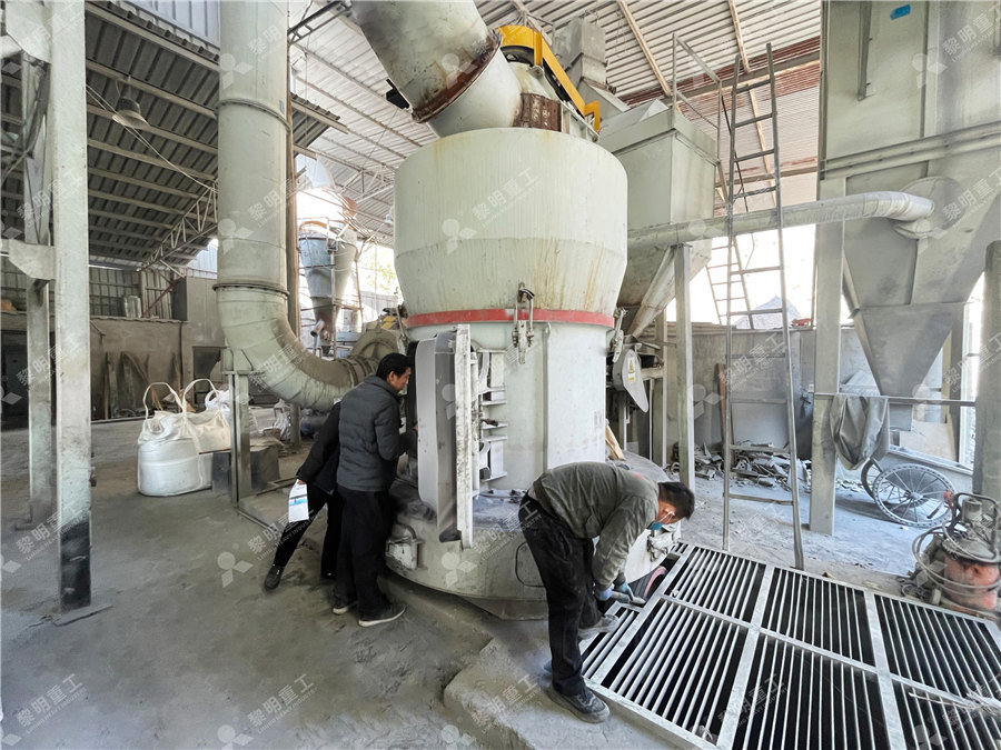
MTW European Type Trapezium Mill
Input size:30-50mm
Capacity: 3-50t/h
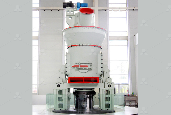
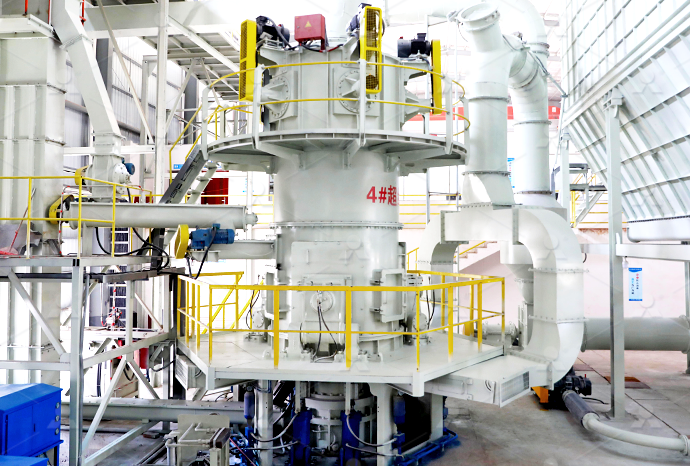
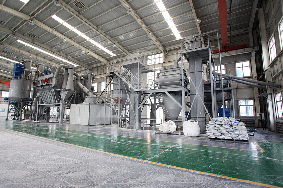
LM Vertical Roller Mill
Input size:38-65mm
Capacity: 13-70t/h
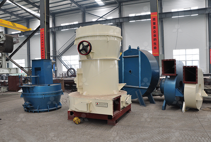
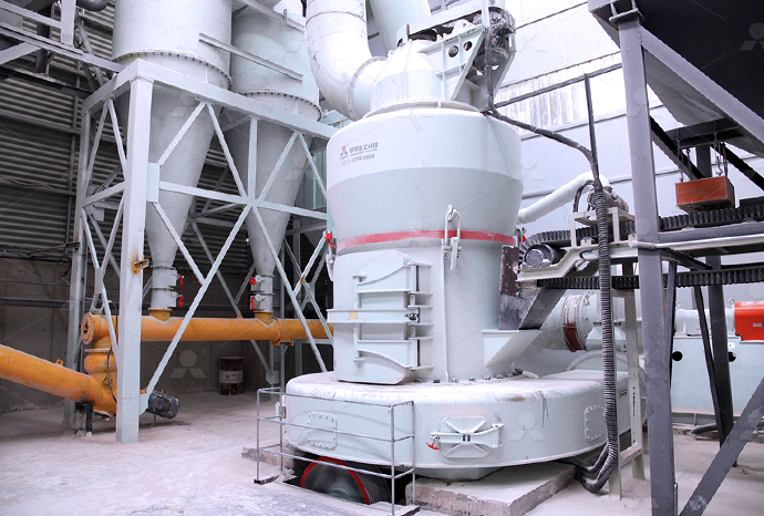
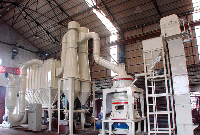
Raymond Mill
Input size:20-30mm
Capacity: 0.8-9.5t/h
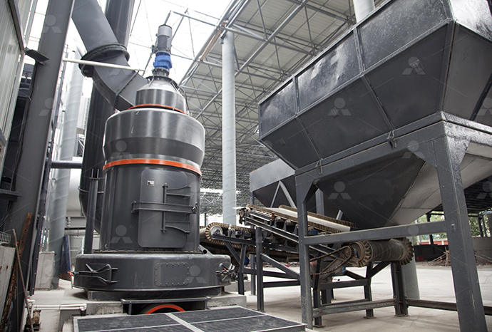
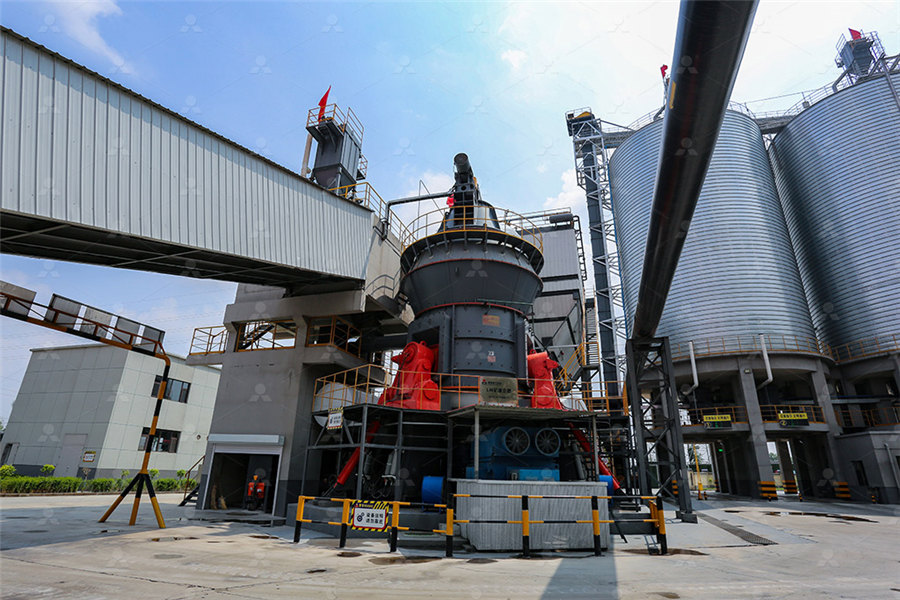
Sand powder vertical mill
Input size:30-55mm
Capacity: 30-900t/h
LUM series superfine vertical roller grinding mill
Input size:10-20mm
Capacity: 5-18t/h
MW Micro Powder Mill
Input size:≤20mm
Capacity: 0.5-12t/h

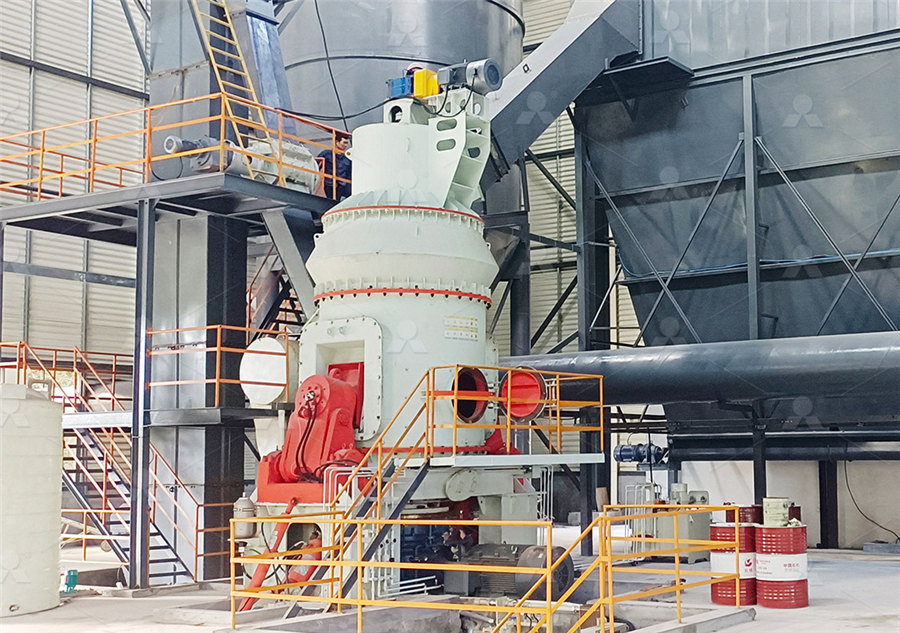
LM Vertical Slag Mill
Input size:38-65mm
Capacity: 7-100t/h
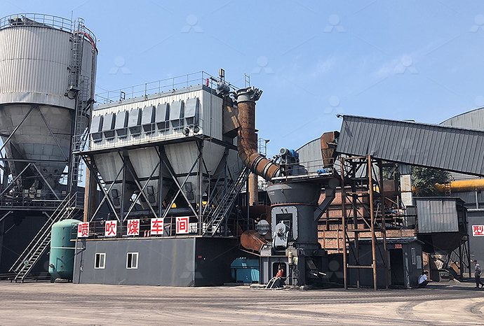
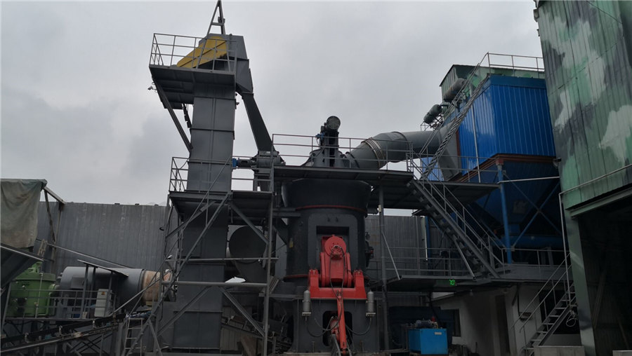
LM Vertical Coal Mill
Input size:≤50mm
Capacity: 5-100t/h
TGM Trapezium Mill
Input size:25-40mm
Capacity: 3-36t/h
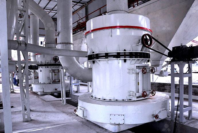
MB5X Pendulum Roller Grinding Mill
Input size:25-55mm
Capacity: 4-100t/h
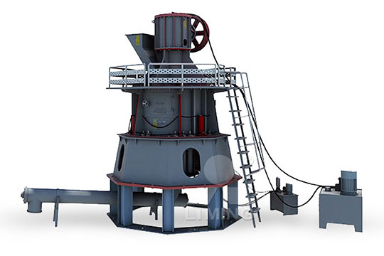
Straight-Through Centrifugal Mill
Input size:30-40mm
Capacity: 15-45t/h
Industrial silicon develops towards deep processing
The transition of energy intensive processing industries towards
2017年11月1日 Energyintensive processing industries (EPIs) produce iron and steel, aluminum, chemicals, cement, glass, and paper and pulp and are responsible for a large share of global 2023年8月3日 The book presents the basic steps and the technical implementation of individual processes for microelectronic circuit integration in silicon Interaction and influences of e g oxidation, etching, doping and Silicon Semiconductor Technology: Processing and 2021年9月1日 In order to realize industrial intelligence in the process industry, it is necessary to deeply integrate industrial AI and the Industrial Internet with the domain knowledge work of the Intelligent Manufacturing for the Process Industry Driven by 2024年9月19日 Researchers at Imec demonstrated superconducting transmon qubits with relaxation and coherence times exceeding 100 microseconds, using a 300mm silicon wafer process The study shows a 9825% yield of functional Researchers: Superconducting Qubit Technology Scales
Scaling siliconbased quantum computing using CMOS technology
2021年12月20日 Recent results in highfidelity control of individual spins in silicon, combined with demonstrations that these qubits can be manufactured in a similar fashion to fieldeffect Silicon Devices and Process Integration covers stateoftheart silicon devices, their characteristics, and their interactions with process parameters It serves as a comprehensive Silicon Devices and Process Integration: Deep Submicron and 2015年10月19日 Taking advantage of small size and large surface to volume ratio of nanomaterials, we develop a scalable and lowcost nanopurification process to produce and Nanopurification of silicon from 84% to 99999% purity with a 2024年5月23日 Designing superior semiconductors and optimizing device fabrication processes are considered crucial for the future development of electronics To address the wellknown Designing semiconductor materials and devices in the post
A Review of Femtosecond Laser Processing of Silicon
2024年5月10日 Silicon carbide (SiC) is a promising semiconductor material as well as a challenging material to machine, owing to its unique characteristics including high hardness, superior thermal conductivity, and chemical 2021年2月26日 These include image classification in industrial IoT [42], smart security [4], smart vehicles [43], edge based speech commands processing [10], and smart health applications such as Toward Deep Transfer Learning in Industrial Internet of Things2020年5月1日 Request PDF Toward EdgeBased Deep Learning in Industrial Internet of Things With the same processing technology (28 nm process) as TrueNorth, Toward EdgeBased Deep Learning in Industrial Internet of 2020年12月1日 High efficiency multicrystalline silicon (mcSi) solar cells with the passivated emitter and rear cell (PERC) technology have been commercialized in the past years [1]One critical issue of the PERC cells is the efficiency degradation under illumination, among which the light and elevated temperatureinduced degradation (LeTID) has been shown to cause >10% Evolution of LeTID defects in industrial multicrystalline silicon
.jpg)
Silicon Semiconductor Technology: Processing and Integration of
2023年8月3日 Interaction and influences of e g oxidation, etching, doping and thermal processes for integrating CMOS and Bipolar circuits are discussed in detail, beginning with the purification of silicon up to the encapsulated integrated circuit2023年12月14日 Technology for 5G 6G infrastructure, satcom, radar for UAV detection and other applications uses existing cleanrooms with larger substrates CEALeti has developed a 200mm gallium nitride/silicon (GaN/Si) process technology compatible with CMOS cleanrooms that preserves the high performance of the semiconductor material and costs less than CEALeti Develops CMOSCompatible 200mm Process Industrial 2021年4月6日 Currently, a growing number of mature natural language processing applications make people's life more convenient Such applications are built by source code the language in software engineering However, the applications for understanding source code language to ease the software engineering process are underresearchedCodeTrans: Towards Cracking the Language of Silicon's Code2022年5月1日 Screen printed crystalline silicon (Si) solar cell panels continue to dominate the global installation of photovoltaic (PV) modules with a market share of about 95% [1]Multicrystalline silicon (mcSi) and mono crystalline silicon (cSi) wafer based solar cells contribute ∼ 30% and ∼ 65%, respectively to the world wide PV panel installation [1]Etching methods for texturing industrial multicrystalline silicon
Towards largescale programmable silicon photonic chip for
2024年2月19日 Here, recent progress of largescale programmable silicon photonic chip for signal processing in microwave photonics, optical communications, optical computing, quantum photonics as well as DOI: 101016/jsolmat2022 Corpus ID: ; Towards an industrial inline solution for efficient posttreatment of silicon heterojunction solar cells @article{Veirman2022TowardsAI, title={Towards an industrial inline solution for efficient posttreatment of silicon heterojunction solar cells}, author={Jordi Veirman and JeanSol Caron and Philippe Jeronimo and Tristan [PDF] Towards an industrial inline solution for efficient post 2021年1月15日 Screen printing technology is the dominant metallization process for industrial silicon wafer solar cells and is also a wellestablished process for contacting phosphorus diffused emitters Previously, screenprinted Ag pastes required heavily doped phosphorus emitters to achieve a good ohmic contact, and this in turn directly limited the efficiency of the solar cellsPathways for efficiency improvements of industrial PERC silicon PDF On Jan 1, 2010, B Raabe and others published The development of etchback processes for industrial silicon solar cells Find, read and cite all the research you need on ResearchGate(PDF) The development of etchback processes for
.jpg)
The transition of energy intensive processing industries towards deep
2017年11月1日 Request PDF The transition of energy intensive processing industries towards deep decarbonization: Characteristics and implications for future research Energyintensive processing industries Recent processing advances towards fullwafer twoterminal perovskite/ silicon tandem solar cells Abstract Twoterminal tandem solar cells based on perovskite/silicon (PK/ Si) technology represent one of the most exciting pathways towards pushing solar cell efficiencies beyond the thermodynamic limit of singlejunction crystalline silicon devicesRecent processing advances towards fullwafer twoterminal ARTICLE Controlled strong excitation of silicon as a step towards processing materials at subnanometer precision ThanhHung Dinh1*, Nikita Medvedev 2,3*, Masahiko Ishino1,4, Toshiyuki Kitamura1 Controlled strong excitation of silicon as a step towards processing jective is to reduce the grams of Silicon per Wp by a factor of 2 with an efficiency increase of roughly 20% relative (from 17−18% → >20% for industrial crystalline Si solar cells) [2] 2 Experimental results 21 Efficiency improvement potential: the toolbox application The output efficiency of monocrystalline Silicon soEvolutionary process development towards next generation
Solar grade silicon: Technology status and industrial trends
2014年11月1日 This was enabled by a deep preexisting chemical processing and industrial value chain, and has in turn given rise to the further development of a polysilicon value chain including metallurgical grade silicon/MGS (more than 50% of global MGS capacity is Chinese), TCS, equipment, pipes and vessels, construction competency etc2018年10月4日 The chapter will introduce industrial silicon solar cell manufacturing technologies with its current status Commercial ptype and high efficiency ntype solar cell structures will be discussed and compared so that the reader can get a headstart in industrial solar cells A brief overview of various process steps from texturing to screenprinted metallization is presentedIndustrial Silicon Solar Cells IntechOpen2020年1月1日 Towards Deep Learning in Industrial Applications Taking Advantage of ServiceOriented Architectures Author links open overlay panel Clemens Briese a, Marian Schlüter a, (CNN) have proven very successful in the field of image processing and the recognition and classification of objects [2, 3, 4, 5]Towards Deep Learning in Industrial Applications Taking 2020年9月18日 Silicon gratings with an area of 70 × 70 mm2, pitch size of 12 and 2 μm were fabricated using the optimized process with aspect ratio α of ~67 and 77, respectively SEM images of crosssection Towards the Fabrication of HighAspectRatio Silicon Gratings by Deep
(PDF) Evolutionary process development towards
2012年8月14日 In order to maximize the power output of polycrystalline silicon PVmodules, in previous work we have already tested rectangular cells of 39 × 156 mm which are overlapped along the long sides2021年9月14日 In this work, the authors present a comprehensive review for securing IndustrialIoT (IIoT) devices to contribute to the development of security methods for IIoT deployed over 5G and blockchainRole of Machine Learning and Deep Learning in Batch to batch variability has been an issue for many silicon RD efforts as the surface of silicon is active towards water, air, and organics We have been evaluating silicon scaleup production methods for possible use in the DeepDive program • HEBM of commercial silicon boules leads to the formation of active surfaces during the processingSILICON DEEPDIVE: UPDATE AND OVERVIEW Department of 2014年1月1日 A schematic of the basic structure for a typical stateoftheart industrial cSi solar cell is shown in Fig 13The base is ptype material, moderately B doped to a resistivity of around 1 Ω cm (N A = 1510 16 per cm 3)The emitter is n ++doped 2 using P with high surface concentration N D > 10 20 per cm 3, and the front surface is textured to allow a better StateoftheArt Industrial Crystalline Silicon Solar Cells
.jpg)
Towards CostEffective Novel Ultrathin Crystalline Silicon Wafer
PDF On May 7, 2018, Mona zolfaghari borra and others published Towards CostEffective Novel Ultrathin Crystalline Silicon Wafer Production by UltraFast Laser Deep Subsurface Processes Followed 2019年9月25日 Toward Industrial Exploitation of THz Frequencies: Integration of SiGe MMICs in SiliconMicromachined Waveguide Systems September 2019 IEEE Transactions on Terahertz Science and Technology PP(99):11Toward Industrial Exploitation of THz Frequencies: Integration of 2019年6月19日 These results are the fundamental components to demonstrate a roadmap towards 24% industrial PERPoly (industrial TOPCon) cells SEM micrographs visualizing reduced etching by GEN2 firethrough pastesPolySi Based Passivating Contacts Enabling Industrial Silicon PDF On May 15, 2019, Mehul C Raval and others published Industrial Silicon Solar Cells Processing of silicon wafer after diffusion and edge isolation (a) w hich ha ve deep str aight (PDF) Industrial Silicon Solar Cells ResearchGate
Towards an industrial inline solution for efficient posttreatment
2022年9月1日 Request PDF Towards an industrial inline solution for efficient posttreatment of silicon heterojunction solar cells Light exposure is widely known to enhance the performance of amorphous 2024年5月10日 Silicon carbide (SiC) is a promising semiconductor material as well as a challenging material to machine, owing to its unique characteristics including high hardness, superior thermal conductivity, and chemical A Review of Femtosecond Laser Processing of Silicon 2021年2月26日 These include image classification in industrial IoT [42], smart security [4], smart vehicles [43], edge based speech commands processing [10], and smart health applications such as Toward Deep Transfer Learning in Industrial Internet of Things2020年5月1日 Request PDF Toward EdgeBased Deep Learning in Industrial Internet of Things With the same processing technology (28 nm process) as TrueNorth, Toward EdgeBased Deep Learning in Industrial Internet of
Evolution of LeTID defects in industrial multicrystalline silicon
2020年12月1日 High efficiency multicrystalline silicon (mcSi) solar cells with the passivated emitter and rear cell (PERC) technology have been commercialized in the past years [1]One critical issue of the PERC cells is the efficiency degradation under illumination, among which the light and elevated temperatureinduced degradation (LeTID) has been shown to cause >10% 2023年8月3日 Interaction and influences of e g oxidation, etching, doping and thermal processes for integrating CMOS and Bipolar circuits are discussed in detail, beginning with the purification of silicon up to the encapsulated integrated circuitSilicon Semiconductor Technology: Processing and Integration of 2023年12月14日 Technology for 5G 6G infrastructure, satcom, radar for UAV detection and other applications uses existing cleanrooms with larger substrates CEALeti has developed a 200mm gallium nitride/silicon (GaN/Si) process technology compatible with CMOS cleanrooms that preserves the high performance of the semiconductor material and costs less than CEALeti Develops CMOSCompatible 200mm Process Industrial 2021年4月6日 Currently, a growing number of mature natural language processing applications make people's life more convenient Such applications are built by source code the language in software engineering However, the applications for understanding source code language to ease the software engineering process are underresearchedCodeTrans: Towards Cracking the Language of Silicon's Code
Etching methods for texturing industrial multicrystalline silicon
2022年5月1日 Screen printed crystalline silicon (Si) solar cell panels continue to dominate the global installation of photovoltaic (PV) modules with a market share of about 95% [1]Multicrystalline silicon (mcSi) and mono crystalline silicon (cSi) wafer based solar cells contribute ∼ 30% and ∼ 65%, respectively to the world wide PV panel installation [1]2024年2月19日 Here, recent progress of largescale programmable silicon photonic chip for signal processing in microwave photonics, optical communications, optical computing, quantum photonics as well as Towards largescale programmable silicon photonic chip for DOI: 101016/jsolmat2022 Corpus ID: ; Towards an industrial inline solution for efficient posttreatment of silicon heterojunction solar cells @article{Veirman2022TowardsAI, title={Towards an industrial inline solution for efficient posttreatment of silicon heterojunction solar cells}, author={Jordi Veirman and JeanSol Caron and Philippe Jeronimo and Tristan [PDF] Towards an industrial inline solution for efficient post